Nets
You can design boards simply by placing footprints, pads and traces, however taking a little extra time to create circuit nets can save countless hours later.
Nets indicate which pads should be connected to each other without specifying the specific path of traces. It is highly recommended to create Nets because they can:
- save hours of debugging
- reduce errors
- help you optimize the board layout
- simplify routing traces
- allow use of the Auto Router
- let you check your board for errors automatically
- make it far easier to later change your layout
- Using the Logical Connections (best if you generally work directly with a PCB layout instead of doing a circuit diagram first).
- Manually, using the Edit Nets Dialog.
- Via the Import Netlist capability.
Logical connections
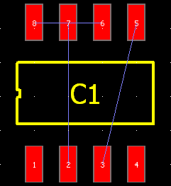
Logical connections are thin blue lines that specify which pads are to be electrically connected prior to creating traces that actually make the connections.
For example, in the illustration below, pins 2, 6, 7, 8 are one set of logical connections (one net), which means they are to be connected with traces. Pins 3 and 5 are another logical connection or net. Pins 1 and 4 are not logically connected to any other pins, so their net is Empty.
 You can make a logical connection between any pads. For example, you might want to make a logical connection between pin 12 of an integrated circuit and pin 1 of a resistor.
 You can make a logical connection between any pads. For example, you might want to make a logical connection between pin 12 of an integrated circuit and pin 1 of a resistor.
To make logical connections (to make a net):
You can change which logical connection net a pin belongs to. For example you might decide that a certain pin of an IC should not be connected to a clock signal by removing the pin from a net named “Clock”.
- Place footprints and/or pads.
- In the left toolbar select the Logical Connection tool or press the N key.
- Click the first pad to be connected. As you move the mouse you will see a thin line.
- Click the second pad to be connected. A dialog appears.
- Click Enter new name and enter a name for the new net (e.g. “Ground”, “+15V”, “Sensor In”, etc.).
- Click OK.
- If needed click additional pins belonging to the same net.
- When finished, right click.
- If desired, review the nets by choosing Nets | Edit Nets.
To assign a pad to a different Net:
To hide Logical Connection lines uncheck View | Layers | Net layer.
To leave a pin unconnected assign it to the Empty net.
To make sure you have added all needed traces watch for all of the Logical Connections lines to disappear.
To see which pads are unconnected to a specified pad move the Logical Connection tool over the specified pad and watch for highlighted pads.
If you try to connect pins that belong to different nets, a dialog will ask if you want to merge the nets or reassign connected pins.
When you connect two pins with the Logical Connections tool, the line you expect to see may be rerouted, but the electrical connection will be maintained. This occurs because Pad2Pad automatically minimizes the total length of the logical connection lines.
Lastly, double clicking a logical connection line causes the Edit Net dialog to appear and show the net.
- Select the pad.
- On the Property bar select the desired net from the drop list.
- Or use Nets | Edit Nets.
Edit Nets Dialog
The Edit Nets dialog is a dialog that allows you to view, change and delete nets in your design. You use the Edit Nets dialog to define the connections to be made in your circuit board:
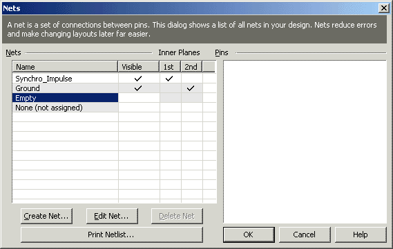 For example you might want to create a net for a clock signal that connects a clock to two ICs.
 For example you might want to create a net for a clock signal that connects a clock to two ICs.
To create a new net:
The “Pins in net:” list may contain grey pins. Grey pins are pins that have electrical contact with the net but don’t belong to the net. Use the Add Grey button to add such pins to the net.
- Choose Nets | Edit Nets and the Nets dialog will appear as shown above.
- Click Create Net
- Type the name of the new net (e.g. Clock, Ground, H4, etc). Click OK.
- On right side of the dialog click on a pin that belongs in the new net and click <. (Click > to remove a pin from a net.) Refer to the circuit schematic during this process.
- Continue to select and move pins until all pins to be included in the net are listed in the “Pins in net” area.
- Click OK.
- You will now see the new net in the main Nets dialog. Click OK.
To edit an existing net:
- Choose Nets | Edit Nets and the Nets dialog will appear.
- Select the net to edit.
- Review pins shown in the “Pins in net” list. The right list contains all pins available on the board excluding those belonging to the selected net.
- To remove a pin from the net, select it and click >
- To add a pin to the net from the right side list, select it and click <. The pin moves to the “Pins in net” list..
- To quickly locate a pin in the list, use the Search for pin field.
- Continue editing nets.
- Click OK when finished.
To delete an existing net:
- Choose Nets | Edit Nets and the Nets dialog will appear.
- Select the net to delete.
- Check the “Delete traces connected to this net” checkbox if you wish the traces to be also deleted.
- Click Delete Net
- Click OK.
To sort the net list by name:
- Click the name column header.
- Click again to reverse sorting.
To print a list of all nets and assigned pins:
- Choose Nets | Edit Nets and the Nets dialog appears.
- Click Print Netlist and the Print dialog appears. Select the desired print settings; click OK.
To change what the internal layers of four layer circuit boards are connected to:
- Create two new nets to be assigned to the two internal layers (ex: MyInternal1 and MyInternal2)
- In the Edit Nets | “1st” column set check mark next to MyInternal1
- In the Edit Nets | “2nd” column set check mark next to MyInternal2
- Note: The 1st internal layer is located under the top copper layer and the 2nd internal layer is located above the bottom layer.
To assign Empty net to all free pins:
- Choose Nets | Edit Nets and the Nets dialog will appear.
- Select Empty net in the Nets list.
- Check Show Free pins only checkbox.
- Click << button.
- Click OK.
To indicate if a net is to be routed by Auto-router:
- Choose Nets | Edit Nets and the Nets dialog will appear.
- Select the net to enable/disable auto-routing for.
- Set check in the Route column to allow auto-routing. Clear check for the Auto-router to completely ignore the net.
- Click OK.
To specify/change trace width for a net to use by Auto-router:
The dialog is modeless. While the dialog is displayed, clicking a pin selects the net of the pin in the dialog.
- Choose Nets | Edit Nets and the Nets dialog will appear.
- Select the net to specify/change trace width for.
- Click the Trace width field. If editing did not start, click the field again.
- Specify/change the trace width.
- Click OK.
Netlist
A netlist is a set of nets, usually created by a circuit design software. You can import netlists from the following industry-standard formats:
- OrCAD
- Protel (also supported by TinyCAD)
- Eagle (also supported by TinyCAD)
- EDIF (supported by popular CAD applications, such as P-CAD and OrCAD)
- PDIF (supported by popular CAD applications, such as P-CAD and OrCAD)
To import a netlist from one of the above formats to Pad2Pad:
- Select the Footprint tool.
- Place all footprints. For custom footprints, use single layer pads or multi layer pads to place separate pads and group them.
- Ensure corresponding components match between your design and the schematic that generated the netlist.
- Choose Nets | Import Netlist and a dialog will appear.
- From Files of Type select the netlist format to import.
- Browse for the netlist file to import; click Open. The Import Netlist dialog will appear.
- Check correctness of the import. Components and pins in the imported netlist (“Original Netlist”) column should correspond to component footprints and their corresponding pads in your design (“Pad2Pad Design”) column. You can reassign the corresponding components and pads, if necessary.
- Click OK to complete the import.
- Choose Nets | Edit Nets or use the Property Bar to review or edit the resulting nets.
- Typically you will then create traces via the Auto Router or manually. But first select View | Layers and enable the Net layer.
Creating Nets from Traces
You can create nets automatically from your traces. This is useful if you created a circuit design by laying traces without first creating nets. A great tool especially prior to rearranging a board layout as the nets will automatically help you avoid errors while rearranging components. The nets will also allow you to use the PCB auto router to perform or help with the rearrangement.
To Create Nets from Traces:
- Click Nets | Create Nets from Traces. Pad2Pad will scan the board layout and create nets. A dialog will appear to tell you how many Nets were created.
- Choose Nets | Edit Nets to review the created Nets. The Nets will be named “Auto01”, “Auto02”, etc.
- Typically you would then enable View | Layers | Net and then proceed with rearranging your circuit board layout.


