Circles
You can add filled or outline circles to your circuit board layout. For example, you can draw circular mounting holes or create a round board.
To draw a circle:
When the Circle tool is selected or when a circular object on the board is selected, use the Property Bar to specify the style, width, layer, location and diameter.
There are two circle styles: filled and outline. On the Board Layer, use solid fill for holes; use outline to specify a round board.
Hole diameter is only determined by the circle diameter, the line width does not have effect, so it’s recommended to select a narrow width (0.01″) to avoid any confusion.
Holes made with the Circle tool are NPTH. If you want PTH holes, use the Multi-layer pad tool.
- On the left toolbar select the Circle tool or press the O key.
- Click at the desired center of the circle.
- Specify the radius by moving the mouse.
- Click to end.
Arcs
You can add arcs to your design. For example, you can draw arc-shaped traces, or create a board with rounded corners.
To draw an arc:
When the Arc tool is selected or when an arc-shaped object on the board is selected, use the property bar to specify the width, layer, location or radius.
- Select the Arc tool or press the A key.
- Click at the start of the arc.
- Click at the end of the arc.
- Specify the radius by moving the mouse.
- Click to end.
Polygons
A polygon is a closed shape with straight edges. You can create polygon shapes on any layer. For example you might create a polygon shape to create a ground plane.
To draw a polygon shape:
- On the left toolbar choose the Polygon tool.
- Choose the desired layer.
- Click at several locations along the shape.
- When finished, right-click.
To remove a node:
- Select the shape.
- Double-click the node to be removed.
To modify a polygon:
- Select the shape.
- Drag a node handle to reshape
To help avoid polygons to self-intersect:
- In the main menu choose Edit | Preferences | PCB Editor.
- Uncheck “Allow self-intersections of polygons”.
Rectangles
You can add outline rectangles to your circuit board layout. For example, you might draw a rectangular slot or footprint outline.
To draw a rectangle:
When the Rectangle tool is selected, use the Property Bar to specify the width and layer. A rectangle drawn with the rectangle tool consists of four traces connected to each other. To change the dimensions after the rectangle is drawn, change the length of the traces.
- On the left toolbar select the Rectangle tool.
- Click at the desired top-left corner of the rectangle.
- Specify the dimensions by moving the mouse.
- Click to end.
Text
You can place text onto your circuit board. For example, you might want to label a resistor “R1”. Text can go on a copper or silk screen layer.
To place text:
- On the left toolbar select the Text tool or press the “T” key.
- On the Property Bar select the Layer where your text is to appear. When placing text on a copper layer (which can save the cost of silk screening) it is recommended to unmask the text for best visibility. To do this, draw a rectangle on the corresponding solder mask layer or copy the same text onto the solder mask layer.
- Click at the desired location for text. The text editor dialog box appears:

-
- Enter the desired text; specify the style parameters; and click OK.
- Text appears at location you selected previously.
- Move the text if needed.
The lock button toggles the lock mode on/off. When the lock mode is ON, the proportion between the font size and the line width is kept automatically.
Line width should be at least 0.007″ to ensure readability.
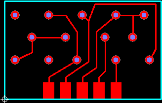
Before
After
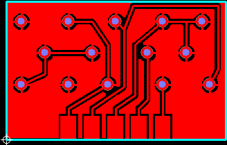
To fill the area between traces with copper and connect objects of your ground net:
- On the left toolbar choose the Polygon or Circle tool.
- On the property bar Layer list select Top or Bottom.
- For clarity turn off the other layers using the layer toolbar button.
- Draw the desired shape and select the shape.
- On the property bar select your ground net from the “Net” drop-down box.
- Choose Tools | Ground Planes | Create and the Ground Plane dialog will appear.
- Enter the desired distance between traces and the fill (described below).
- Click OK.
The polygon object defining the area to fill might overlap a copper object. If the polygon and the other copper object belong to the same net they will get connected.
The Ground Plane Create command must be applied after the traces are routed.
To indicate whether to use thermal or solid connection for a pad:
Before etch copper:
- Click a pad.
- On the property bar click the Additional properties
 button.
 - Choose “Thermal” to force thermal connection or choose “Solid” to force solid connection.
- Click OK.
To delete a plane created by create ground plane:
- Select an object of the plane.
- Choose Tools | Ground Plane | Delete
- Click OK.
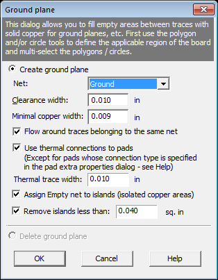
The Thermal trace width parameter specifies the width of traces connecting a copper object to the polygon object when both belong to the same net.
The Ground plane command only works for polygons that are inside the board outline.
